Privacy statement: Your privacy is very important to Us. Our company promises not to disclose your personal information to any external company with out your explicit permission.
With the increasing demand for chips in various fields such as communications equipment, consumer electronics, automotive, etc., the global chip shortage and price increase wave is getting more and more intense. Chip manufacturing process is very complex, when it comes to semiconductor manufacturing, more attention is often paid to silicon wafers, electronic special gas, photomasks, photoresists, targets, chemicals and other materials and related equipment, few people introduced throughout the semiconductor process of the invisible guardian - plastic.
The biggest challenge facing semiconductor manufacturing is the control of pollution, especially with the development of semiconductor technology, electronic components are getting smaller and more complex, the lower the tolerance of impurities, the production of harsh conditions, such as dust-free cleaning, high temperature, highly corrosive chemicals.
Throughout the semiconductor process, the role of plastics is primarily packaging and transport, connecting each processing step, preventing contamination and damage, optimizing contamination control, and improving the yield of critical semiconductor processes. Plastic materials used include PEEK, PPS, PP, ABS, PVC, PBT, PC , fluoroplastics, PAI, COP, etc., and with the continuous development of semiconductor technology, the performance requirements for the material is also increasingly high.
The following focuses on the application of special engineering plastics PEEK/PPS in semiconductor manufacturing.
1, CMP fixed ring
Chemical Mechanical Grinding (CMP) is a key process technology in the wafer production process, CMP fixed ring is used in the grinding process to fix the wafer, wafer, the choice of materials should have good wear resistance, dimensional stability, chemical corrosion resistance, easy to process, to avoid the crystal wafer / wafer surface scratches, pollution.
CMP fixed ring is used to fix the wafer in the grinding process, the material chosen should avoid the wafer surface scratching, pollution, etc., usually using standard PPS production.
PEEK has high dimensional stability, easy to process, good mechanical properties, good chemical resistance and good abrasion resistance, compared with PPS ring, made of PEEK CMP fixing ring is more abrasion-resistant, the service life is doubled, thus reducing the downtime and improving wafer production capacity.
Material: PEEK, PPS

2. Wafer Carriers
Wafer carrier, as the name suggests, is used to load wafers, wafer carrier box, wafer transport box, crystal boat and so on. Wafers stored in the transportation box in the entire production process accounts for a high proportion of the time, the wafer box itself, the material, quality and cleanliness may have a greater or lesser impact on the quality of wafers.
Wafer carriers are generally temperature resistance, excellent mechanical properties, dimensional stability, as well as rugged, anti-static, low outgassing, low precipitation, recyclable materials, different processes used in the wafer carriers selected materials vary.
PEEK can be used to make the general transfer process with carriers, generally used antistatic PEEK, PEEK has many excellent properties, wear resistance, chemical resistance, dimensional stability, antistatic and low outgassing, to help prevent particle contamination and improve the reliability of wafer handling, storage and transfer.
Materials include: PEEK, PFA, PP, PES, PC, PEI, COP, etc., which are generally modified with anti-static properties.

3.Light mask box
Photomask is a chip manufacturing photolithography process used in the graphic master, quartz glass as a substrate and coated with chrome metal shading, the use of the exposure principle, the light source through the photomask projection to the silicon wafer can be exposed to show a specific pattern. Any dust or scratches attached to the photomask will cause deterioration in the quality of the projected image, so it is necessary to avoid contamination of the photomask, and to avoid particles generated by collision or friction that may affect the cleanliness of the photomask.
In order to avoid damage caused by fogging, friction, or displacement of the mask, the mask box is generally made of anti-static, low outgassing, and rugged materials.
PEEK high hardness, very low particle generation, high cleanliness, anti-static, chemical resistance, abrasion resistance, hydrolysis resistance, very good dielectric strength and excellent radiation resistance and other characteristics, in the production, transmission and handling of photomasks in the process of photomasks, so that the photomask sheet can be stored in the low outgassing and low ionic contamination in the environment.
Materials: anti-static PEEK, anti-static PC, etc.

4.Wafer tools
Tools used to clamp wafers or silicon wafers, such as wafer clamps, vacuum wands, etc. When clamping wafers, the materials used will not produce scratches on the surface of the wafer, no residue, to ensure that the surface of the wafer cleanliness.
PEEK is characterized by high temperature resistance, abrasion resistance, good dimensional stability, low outgassing, and low hygroscopicity. When wafers and silicon wafers are clamped with PEEK wafer clamps, there is no scratching on the surface of wafers and silicon wafers, and no residue is generated on wafers and silicon wafers due to friction, which improves the surface cleanliness of wafers and silicon wafers.
Material: PEEK

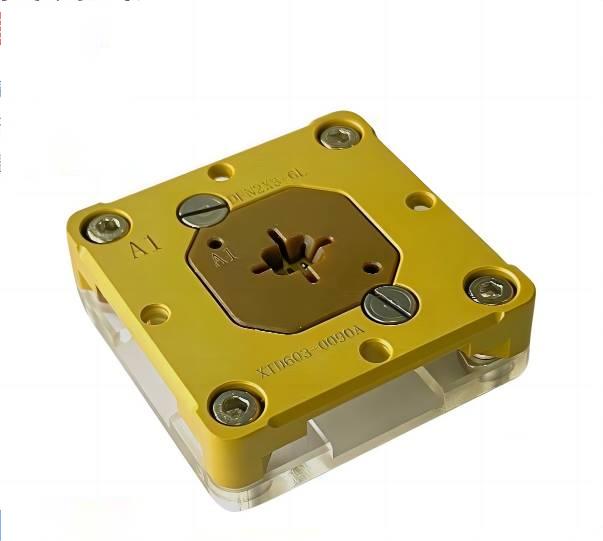
5.Semiconductor package test socket
Test socket is the direct circuit of each semiconductor component electrically connected to the test instrument on the device, the different test sockets are used to test the integrated circuit designers specified by a variety of microchips. The materials used for test sockets should meet the requirements of good dimensional stability over a wide temperature range, mechanical strength, low burr formation, durability, and ease of processing.
Materials: PEEK, PPS, PAI, PI, PEI

LET'S GET IN TOUCH

Privacy statement: Your privacy is very important to Us. Our company promises not to disclose your personal information to any external company with out your explicit permission.

Fill in more information so that we can get in touch with you faster
Privacy statement: Your privacy is very important to Us. Our company promises not to disclose your personal information to any external company with out your explicit permission.